분석실
소재·부품·장비 분야 고도화된 시험분석지원을 통해 도내 중소기업 개발 난제 해결 지원
※ 경기도 수원시 영통구 광교로 145 E동 2층 경기도 반도체혁신센터
보유장비
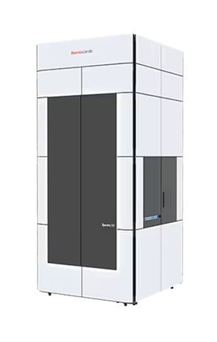
수차보정 투과전자현미경(Cs-TEM)
모델명(제조사)
Spectra 300(Thermo Fissher Scientific)
설치장소
투과전자현미경실(B동 지하1층 105호, BB105)
원리
고전압의 전자빔을 시편에 조사하여 투과된 전자들의 신호를 이미지화 하는 원리. 또한 자기장 렌즈로부터 발생하는 수차에 의한 왜곡을 보정하여 보다 정확한 이미지를 획득
기기활용
1) S/TEM 분석을 통해 광범위한 소재 분야에서 여러 물질들의 구조 이미지 및 결정구조 확인
2) EDS 분석을 통한 화학적 조성비 및 맵핑 이미지를 원자 수준에서 확인
3) EELS 분석을 통한 밴드갭 확인
사양
Dark-field/Bright-field/HR-TEM(resolution<Å) mode
Electron acceleration voltage alignment 60–300 kV (60, 80, 200, 300 kV)
Multi-signal STEM imaging
Cs double-corrector(CETCOR/S-CORR)
담당자
031-888-9433/031-888-9437, kim.hs@snu.ac.kr/shcho90@snu.ac.kr
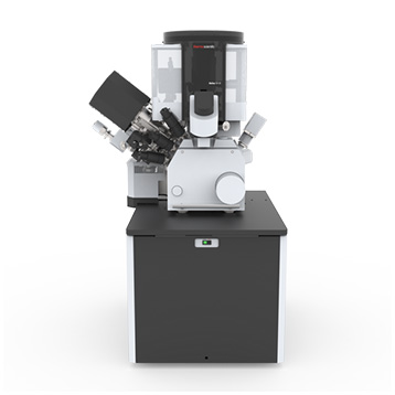
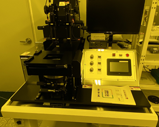
Focused Ion Beam Scanning Electron Microscope 1 (이온빔 주사전자현미경1)
모델명(제작사)
Helios 5 UC (FEI)
설치장소
전자현미경실 (B동 지하 1층)
원리
전자빔을 활용하여 미세 구조물 시료의 표면을 관찰하는 고분해능 현미경으로 표면 형태, 구조 등 관찰
높은 가속전압을 가해 이온을 발생시키고 표면의 선택적 영역에 주사하여 시료를 가공
기기활용
높은 Ion beam 밀도로 빠른 속도의 FIB 시료 가공 가능
저 가속 전압 샘플 가공이 용이하여 고품질의 TEM 샘플 제작 가능
EDX detector 추가를 통하여 표면 원소성분 분포, 정성 및 정량 분석 가능
반도체, 디스플레이의 미세 구조, 패터닝 등의 분석에 활용 가능
사양
1) FIB/FE-SEM
Resolution
High resolution : 0.6nm at 30kV (STEM), 0.6nm at 15kV, 1.7nm at 1kV
Coincident Point (WD 5mm) : 1.2nm at 1kV
Acceleration voltage range : 0.02 ~ 30kV
Probe current : 5pA to 20nA
Magnification range : 12✕~2,000,000
Electron Source : Schottky field emitter
Focus Working Distance : 1~40mm
Beam Shift (at 20kV, WD=8.5mm) : 100㎛(±50㎛)
2) FIB column
Ion Source : Gallium Liquid Ion Metal source
FIB resolution : 2.5nm at 30kV
Probe Current : 1pA to 100nA
Magnification : 300✕~500,000
Acceleration Voltage : 0.5 ~ 30kV
3) Detector
TLD : Efficient detection of SEs, Low take off angle BSEs
MD : Medium take-off angle BSEs – better materials contrast
ICD : High take-off angle, Low-loss BSEs - pure materials contrast
4) Software
AutoTEM 5, AutoTEM 5 Automation Science, Enhanced Stage Rotation Accuracy, AutoSlice and View 4, AutoSlice and View Analytical Package, Maps 3 for SEM
5) EDS
EDS-Quantax 400 XFlash 6-30mm2 – 129eV – Quantax 400 Q655-30-129
담당자
031-888-9434, lanjoo@snu.ac.kr
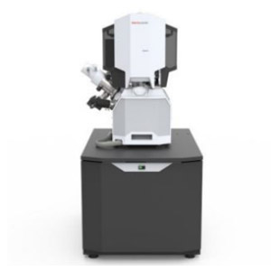
Focused Ion Beam Scanning Electron Microscope 2 (이온빔 주사전자현미경2)
모델명(제작사)
Scios2 (FEI)
설치장소
전자현미경실 (B동 지하 1층)
원리
Electron 및 Ion 의 두 개의 column으로 이루어진 Dual Beam system이 적용된 장비이며, Ga source를 활용한 집속 이온 빔의 식각 특성을 활용하여 Sub-Micro & Sub-Nano의 미세 영역을 가공 및 분석하는 장비
특정 영역의 가공 및 이미지 관찰이 용이하며 가공한 샘플을 chamber 내부에서 SEM을 활용 하여 직접적으로 imaging 분석 및 EDS를 활용한 성분분석.
기기활용
Sidewinder HT 이온 컬럼을 통한 고품질, 위치별 TEM 시료 제작 가능
높은 Ion beam 밀도로 빠른 속도의 FIB 시료 가공 가능
EDX detector 추가를 통하여 표면 원소성분 분포, 정성 및 정량 분석 가능
반도체 및 디스플레이 장치를 이미지화 및 특성 분석
사양
1) FIB/FE-SEM
High resolution : 0.7 nm at 30 kV (STEM), 1.0 nm at 30 kV, 1.4 nm at 1 kV
Acceleration voltage range : 0.02 ~ 30 kV
Probe current : 1 pA to 400 nA
Magnification range : 12~1,250,000×
Electron source : Schottky field emitter
Focus working distance : 1~40 mm
2) FIB column
Ion source : Gallium Liquid
Ion Metal source
FIB resolution : 3.0 nm at 30 kV
Probe current : 1.5 pA to 65 nA
Magnification : 300~500,000×
Acceleration voltage : 0.5 ~ 30 kV
3) Detector
• Trinity Detection System
- T1 : segmented lower in-lens detector (BSE)
- T2 : upper in-lens detector (SE)
- T3 : retractable in-column detector (SE)
- Up to four simultaneously detected signals
- Angular and energy-selective SE and BSE imaging
• ETD : SE (tunable energy) / BSE
• ICE : electron beam (SE / BSE), ion beam (SE / SI)
4) Software
iSPI, intermittent SEM imaging and FIB patterning iRTM, integrated real time monitor for real-time SEM and FIB process monitoring and endpointing iFast, advanced utomation suite for DualBeam instruments
5) EDS
Quantax 400 XFlash® 6
Active area: 60 mm²
Energy resolution: 129 eV standard
Input count rate: Over 1,500 kcps
Output count rate: Up to 600 kcps
담당자
031-888-9434, lanjoo@snu.ac.kr
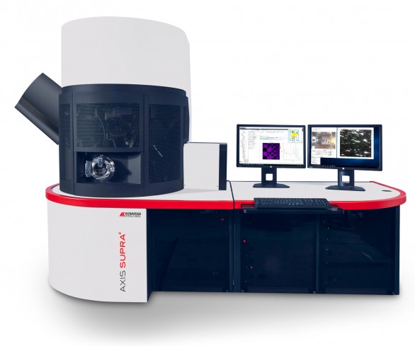
High-performance X-ray photoelectron spectroscopy (고성능 X-선 광전자 분광분석기)
모델명(제작사)
AXIS Supra+ (Kratos, U.K.)
설치장소
X-선 분석실 (C동 B104호)
원리
X-선을 시료 표면에 조사하여 광전효과에 의해 방출된 내각전자의 운동에너지를 측정하여, 원소의 조성 및 화학 결합 상태에 대한 정보를 분석
기기활용
고분자, 유기물, 반도체 등 다양한 물질의 표면 및 계면 분석, 정량 분석, 전자구조 분석
1) XPS : 1,000~1,500 eV의 X-선을 이용하여, 코어레벨의 전자를 분석해 내각전자의 결합에너지, 화학결합상태, 상대 정량 분석
2) UPS : 10~20 eV의 자외선을 이용하여 밸런스 레벨의 전자를 분석해 최외각 전자에너지, 밴드갭 에너지, 일함수 분석
3) ARXPS : 각도 변환에 따른 광전자 분석을 통해 비파괴 수직적 화학 조성 및 분포 분석
4) Temperature dependence : +800℃~-100℃(액체질소) 범위에서의 XPS 분석
5) Depth profile : 이온건을 이용한 시료 에칭을 통해 깊이 분포에 따른 XPS 스펙트럼 측정
사양
1) Electron analyzer with lens system
Type : spherical sector analyzer
Minimum analysis area : 15 μm, 6,000 cps @ 0.6 eV FWHM
Kinetic energy range : 0~1486 eV (Al), 0~2984 eV (Ag)
Ultimate energy resolution of Ag 3d5/2 peak: ≤0.48 eV FWHM
Detector : 128-channel DLD(Delay-Line Detector) with MCP(Micro-Channel Plate)
Maximum sensitivity at 0.6 eV FWHM on Ag3d5: 2,500,000 cps
2) Micro-focused monochromated X-ray source
Anode material : Al (Ag option)
Rowland circle : 500 mm
Automatic control : full data system control and adjustment
Source : Al-Kα (1486.6 eV)
Energy Resolution : Ag 3d5/2
3) Ultra violet light source
Sensitivity : 1,000,000 cps for Ag 4d
HeⅠ(21.2 eV) or He Ⅱ(40.8 eV)
Energy resolution : 110 meV
Minimum step size is 1 meV
4) Sputtering ion gun control
Type : mono Ar and Ar cluster ion source
Ultimate vacuum : 5 × 10⁻⁷ Torr
Beam Energy : 500 eV ~ 4 keV
5) High precision manipulator (5-axis manipulator)
Maximum specimen dimensions : 60 mm dia
Mounting plates: multi-specimen:2, powder: 1
Sample tilt : +, - 45 degree
6) Vacuum transfer holder
Sample holder allowing samples to be transferred under vacuum into the system
Maximum specimen thickness : 9 mm
Three transfer holders
비고
예약 전날 오후 2시까지 샘플 전달(샘플 전달 늦을 시 분석 하루 지연)
Normal/UPS/ARXPS → 시료 1개(1point) 원소 5개당 1시간 소요
Temperature dependence/Depth profile → 분석 소요시간 담당자 문의
담당자
031-888-9443, juhyun.lee@snu.ac.kr
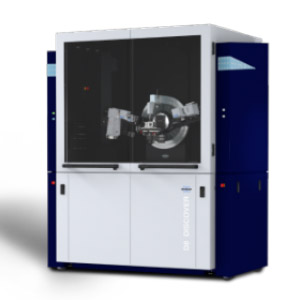
X-Ray Diffraction (X-선 회절 분석기)
모델명(제작사)
D8 Discover (Bruker)
설치장소
X-선 분석실 (C동 B104호)
원리
X선 회절 현상을 이용하여 물질의 결정상 분석, 미지시료의 정성분석, 혼합시료의 정량분석, 결정화도, 격자변형 분석
기기활용
1) XRD, GIXRD, XRR 측정을 통한 물질 상분석, 구조분석, 박막 두께 분석
2) In-situ 온도 XRD: -190~600 ℃ (사전협의 필요)
3) In-situ 전기화학 XRD: 코인셀 충방전에 따른 XRD 측정 (사전협의 필요)
사양
- Available anodes: Cu, Mo
- Goniometer accuracy: Δ2θ ≤ 0.007° determined on NIST SRM 1976X
- Beam divergence: <0.023° at 40 mm
- TRIO Optics
: Software push-button switch between
: Motorized Divergence Slit (Bragg-Brentano)
: High Intensity Parallel Beam
- High-Resolution Monochromators
: Ge(220) and Ge(004) reflection2-bounce monochromator
- Detector
: Active area: 2978 mm²
: Maximum count rate: 3.6×10⁸ ph/s/mm²
: Spatial resolution: 75 μm
: Optimize for γ or 2θ coverage: 0°/90° switchable
: Multi-mode (0D/1D/2D) detector based on the hybrid photon counting
- In-situ XRD
: Temperature: -190 to 600 ℃ (LN₂)
: Electrochemical potential: ±1 A to ±10 mA (resolution: 0.004 %)/±2.5, 5, 10 V(resolution: 0.0015%)
- Pathfinder plus optics
: Software push-button switch between:
: Motorized Slit
: 2-bounce Ge Analyzer
: Automated absorber integrated
- Powder stage
: 9 rotational powder stage (automated)
- Vacuum chuck stage
: x,y for sample translation of up to +/- 150 mm
: z-Drive with travel of up to 50 mm
: Phi drive with infinite rotation
: Max. Psi inclination up to 55°
- Centric Eulerian Cradle (CEC)
: Five degrees of freedom sample stage:
: x,y for sample translation of +/-40 mm
: z-Drive for height alignment
: Phi drive with 360° rotation
: Psi drive and angular range from -11° to 98°
: Various stage attachment available.
담당자
031-888-9443, juhyun.lee@snu.ac.kr
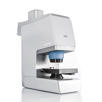
Fourier transform infrared spectroscopy, Microscope (푸리에변환 적외선 분광기, 현미경)
모델명(제작사)
LUMOS II (Bruker)
설치장소
열광학분석실(E동 1층)
원리
적외선에 대한 투과율 및 반사율 측정을 통해 재료의 기능기를 확인하고, 이를 통해 유기 및 무기 화합물의 구조 분석
기기활용
고유 에너지 준위로 인한 흡수 스펙트럼을 통해 물질의 정성분석이 가능하여 wafer, 박막, 소재 분석 등에 활용
사양
Wavenumber range(cm-1) : 6,000~670
Detector : TE-MCT
Spectral resolution (cm-1) : 2(option 0.8)
Signal-to-noise (4cm-1, resolution) : >1,800:1
Spatial resolution : 1.25㎛
Mapping : < 5 spectra/sec (@4cm-1)
Imaging : > 550 spectra/sec (@4cm-1)
Wavenumber accuracy (cm-1) : ≤0.05 (@1,576cm-1)
Beam splitter : ZnSe (optional KBr)
Imaging pixel size : 5㎛ (TR/Refl), 1.25㎛ (ATR)
Objective : 8x
Numerical aperture (15x) : 0.6
Positioning accuracy (at measurement point) : ±0.1㎛
Repeatability : < 0.1㎛
Software : 라이브러리(27만개), 다성분분석 가능, 정량분석 가능
담당자
031-888-9442, lanjoo@snu.ac.kr
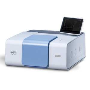
Fourier Transform Infrared Spectroscopy, Bench top(푸리에변환 적외선 분광기, 벤치탑)
모델명(제작사)
INVENIO R (Bruker)
설치장소
열광학분석실(E동 1층)
원리
적외선에 대한 투과율 및 반사율 측정을 통해 재료의 기능기를 확인하고, 이를 통해 유기 및 무기 화합물의 구조 분석
기기활용
고유 에너지 준위로 인한 흡수 스펙트럼을 통해 물질의 정성분석이 가능하여 wafer, 박막, 소재 분석 등에 활용
사양
Wavenumber range(cm-1) : 8,000~340
Detector : Temperature controlled DTGS
Spectral resolution (cm-1) : 0.4
Signal-to-noise (4cm-1, resolution) : >60,000:1
Wavenumber accuracy (cm-1) : ≤0.01 (@1,554cm-1)
Wavenumber precision (cm-1) : ≤0.0005 (@1,554cm-1)
Beamsplitter : KBr
Temporal resolution : Up to 25 spectra per second(@16cm-1 spectral resolution)
Software : 라이브러리(27만개), 다성분분석 가능, 정량분석 가능
담당자
031-888-9442, lanjoo@snu.ac.kr
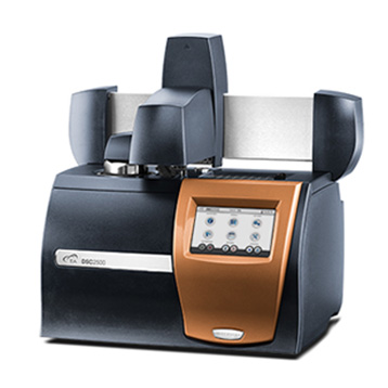
Differential Scanning Calorimetry (시차주사열량분석기)
모델명(제작사)
DSC 250 (TA Instruments)
설치장소
열광학분석실(E동 1층)
원리
온도의 변화에 따른 재료의 물리/화학적 특성변화를 관찰하는 열분석기기로 용융/결정화 엔탈피, 유리전이온도, 열적 안정성, 비열 등 분석
기기활용
다양한 산업에서 활용되는 소재에 대한 열적 특성분석 활용 가능
사양
Sensor type : Heat flux plate
Temperature Range : -90 ~ 400℃
Heating rate : 0.01 ~ 100℃/min
Cooling rate : 0.01 ~ 30℃/min
Enthalpy precision : ±0.08%
Temperature accuracy : ±0.05℃
Temperature precision : ±0.008℃
Calorimetric dynamic range : ±200mW
Automatic gas changer & Mass flow controller : Standard (내장형)
Auto-sampler : 54 sampler
Software : TA universal Software
담당자
031-888-9442, lanjoo@snu.ac.kr
Thermogravimetric Analyzer (열중량분석기)
모델명(제작사)
TGA 8000 (Perkin Elmer)
설치장소
열광학분석실(E동 1층)
원리
온도의 변화에 따른 재료의 물리/화학적 특성변화를 관찰하는 열분석기기로 재료의 열/산화 안정성, 분해속도, 수분함유량 등의 분석
기기활용
다양한 산업에서 활용되는 소재에 대한 열적 특성분석 활용 가능
사양
Balance sensitivity : 0.1μg
Capacity : 1300mg
Balance accuracy : Better than 0.02%
Balance precision : 0.001%
Temperature range : -20℃ to 1200℃
Temperature precision : ±1℃
Scan rates : 0.1℃/min to 500℃/min
Cooling method : Forced air cooled with an external fan
Cooling Cycle time : 1100℃ to 50℃ < 13min
Vacuum : 10-5 Torr
Software : AutoStepwise TGA, Variable rate TGA, TGA Desomposition Kinetics
담당자
031-888-9442, lanjoo@snu.ac.kr
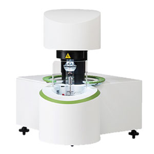
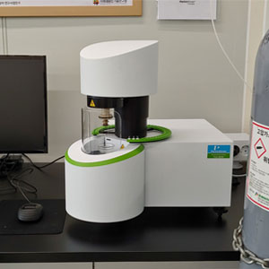
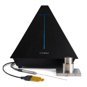
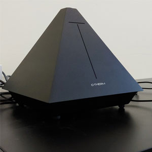
Thermal Conductivity Instrument (열전도율 측정기)
모델명(제작사)
Trident (C-Therm)
설치장소
열광학분석실(E동 1층)
원리
소재 및 물질의 열전도율, 열확산율을 정밀하게 측정하는 분석기기로 열전도율-열확산율을 동시에 측정가능하며, 단위체적당 열용량 등 분석
기기활용
다양한 산업에서 활용되는 소재 및 제품에 대한 방열 및 열적 특성분석 활용 가능
사양
1) MTPS
Thermal conductivity range : 0 to 500W/mK
Thermal effusivity range : 5 to 40,000Ws½/m²K
Temperature range : 50℃ to 200℃ (With option to extend to 500℃)
Precision : better than 1%
Accuracy : better than 5%
Test time : 0.8 to 3 seconds
Sensor size : 18mm diameter
2) Flex TPS
Thermal conductivity range : 0.03 to 500W/mK
Temperature range : 50℃ to 300℃
Precision : better than 2%
Accuracy : better than 5%
Test time : 10 to 180 seconds
Sensor size : 6mm, 13mm and 30mm diameter sensors available
담당자
031-888-9442, lanjoo@snu.ac.kr
Thermal Evaporator
모델명(제작사)
자체 제작
설치장소
클린룸(D동 B101호)
원리
Source 물질을 텅스텐 보트 위에 올린 후 전류를 흘려주어 저항 열을 발생시키면, 그 저항 열에 의해 Source 물질이 증발하게 되어 기판 위에 증착된다.
기기활용
소재부품 시편 제작 및 공정 가능
사양
Align 모듈 개조
Heating system
2 evaporation sources
Highly accurate quartz crystal thickness monitor system
비고
[상태] Air-line 단선
담당자
031-888-9589, lhj6115@snu.ac.kr
Sputtering system
모델명(제작사)
자체 제작
설치장소
클린룸(D동 B101호)
원리
이온화된 물질은 극성을 가지고 있기 때문에 전압을 인가해 이온을 가속시켜 충분한 운동 에너지를 가진 이온을 충돌 시켜 원하는 물질을 떼어내는 방식
기기활용
소재부품 시편 제작 및 공정 가능
사양
3인치 Cathode 3개
3인치 이온건 1개
RF 파워 2SET
DC 파워
비고
[상태] Air-line 단선
담당자
031-888-9589, lhj6115@snu.ac.kr
Mask Aligner/Exposure
모델명(제작사)
Prowin, M150S
설치장소
클린룸(D동 B101호)
원리
도포 및 건조된 PR 위에 UV를 마스크를 통해 전사하여 소자 패터닝이 가능한 장비 기기활용: UV 마스크 정렬 및 노광을 통한 소자 미세 패터닝
기기활용
소재부품 시편 제작 및 공정 가능
사양
조각 시편
4/6인치 웨이퍼
5/7인치 마스크
정렬 정확도 1μm 프리즘 및 2개의 카메라를 통한 동시 정렬 가능
비고
담당자
031-888-9589, lhj6115@snu.ac.kr
Wet station
모델명(제작사)
Prowin, 주문제작
설치장소
클린룸(D동 B101호)
원리
유압 밸브 컨트롤을 통해 현상, 세정 등 웨이퍼 처리가 가능한 장비
기기활용
웨이퍼 세정, 현상, 건조 등 습식 반도체 공정
사양
화학 배스1
린스 배스1
퀵드로우 배스1 (Teflon coated SUS)
비고
담당자
031-888-9589, lhj6115@snu.ac.kr
Probe station / 4-Probe system
모델명(제작사)
MS-tech, M6VC
설치장소
클린룸(D동 B101호)
원리
3개의 Source Measurement Unit, Switching matrix가 연결된 probe station을 이용해 다양한 목적의 소자, 소재 분석이 가능한 장비
기기활용
반도체/디스플레이 소자의 저압-전류 특성 측정
사양
전류 측정 범위 (10 pA ~ 10 mA)
진공 (10-6 torr)
온도 조절 (-196 ~ 296°C) 가능
비고
담당자
031-888-9589, lhj6115@snu.ac.kr
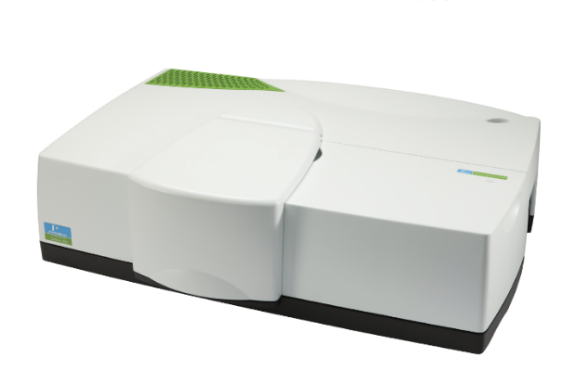
UV-VIS-NIR spectrometer
모델명(제작사)
Lambda 1050+ (Perkin Elmer)
설치장소
오픈랩II (B동5층)
원리
시료가 흡수, 투과, 반사하는 빛의 특정 파장 범위를 측정
기기활용
광학적 투과 반사 흡수 특성 측정
사양
Wavelength range - 175 ~ 3,300 nm
UV-Vis Resolution - ≤ 0.05 nm
NIR Resolution - ≤ 0.2 nm
Wavelength - UV/Vis ± 0.080 nm
Accuracy - NIR ± 0.300nm
Wavelength - UV/Vis : ≤ 0.010 nm
NIR : ≤ 0.040 nm
비고
150 mm Integrating Sphere
담당자
031-888-9589, lhj6115@snu.ac.kr
Potentiostat
모델명(제작사)
Autolab PGSTAT302N
설치장소
오픈랩II (B동5층)
원리
전극들이 담겨있는 셀의 저항을 감지하여 셀 전반의 전위를 제어하고 그 시스템에 공급되는 전류를 변화시켜서 전기회로를 구성하는 방식
기기활용
소재의 전기화학적 특성 분석
사양
측정 가능 교류 주파수 범위 (10 µHz ~ 32 MHz)
인가 전압 범위 (10 V)
비고
담당자
031-888-9568, osjeon@snu.ac.kr
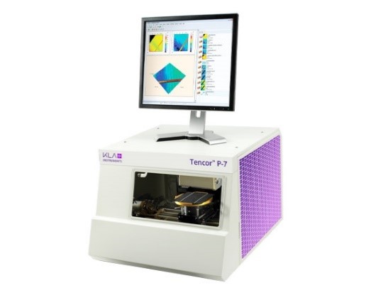
Alpha step
모델명(제작사)
P-7 (KLA)
설치장소
오픈랩2(B동 5층)
원리
탐침이 샘플의 표면을 접촉하여 지나가며 표면의 단차 변화를 측정
기기활용
표면 단차 측정
사양
step height: Nanometers to 1000 μm
Low force with constant force control:0.03 to 50 mg
Video: 5MP high-resolution color camera
비고
담당자
031-888-9589, lhj6115@snu.ac.kr
Nuclear magnetic resonance spectrometer (핵자기공명분광기)
모델명(제작사)
AVANCE III HD 600 MHz NMR Spectrometer (Bruker)
설치장소
분석실 III (C동 B109호)
원리
자기장 조건하에서 시료의 원자핵이 특정 주파수의 전자기파와 공명을 일으키는 현상을 활용하여 시료의 분자 구조를 분석
기기활용
복잡한 화합물들을 단시간에 쉽게 분석가능하며 다양한 유기재료 분석에 활용가능
사양
Frequency resolution : < 0.005Hz
Phase resolution : < 0.006°
Attenuation resolution / attenuation range : < 0.1dB / 90dB
Amplitude modulation : > 90dB
Event time for digital setting of frequency, phase and amplitude, either individually or simultaneously : 25ns
Memory per channel e.g. for pulse shaping : > 8 Mbyte
Phase monotony over 90dB amplitude setting range : < + / -0.5°
담당자
031-888-9434, lanjoo@snu.ac.kr